122b Three Dimensional Inorganic Nanoarrays Created by Electrodeposition through a Crystalline Protein Monolayer
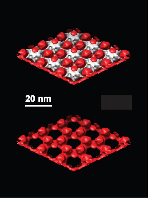
Three dimensional transmission electron microscopy (3D-TEM) is used to characterize the structure of materials electrodeposited through a monolayer of the hexagonally-packed intermediate (HPI) layer protein from D. radiodurans. The crystalline protein monolayers were prepared on unique TEM-compatible electrodes using methods and materials described previously.[1-5] Moderate pH electrodeposition baths (4≤pH≤11) were necessary to preserve the crystalline protein structure. The TEM tilt series data and 3D reconstruction was performed at the National Resource for Automated Molecular Microscopy at Scripps. The abstract figure shows 3D-TEM reconstruction data for cuprous oxide electrodeposited through the crystalline protein monolayer. The top image shows electron density contours that represent the inorganic deposit (red) and the protein template (white). Here the inorganic material is electrodeposited cuprous oxide. The electrodeposited material grows through the pores in the protein as a hexagonal nanoarray, with the larger cuprous oxide particle organized with 3-fold symmetry and smaller particles on top of the 6-fold protein sites. The bottom image shows the 3D architecture of the electrodeposited material by itself, with the protein removed. One sees that each of the large cuprous oxide particles sits on a thin, fully interconnected hexagonal lattice on the substrate. The protein itself is largely invisible to the electron beam, so its structure is revealed as a negative replica of the electron-dense inorganic materials. The fact that the protein structure we observe closely matches previous studies, demonstrates that the 3D pore structure in HPI-layer protein is fully accessible to electrodeposition. Moreover, we show that electrodeposition of complex inteconnected structures is possible below 10 nm, augering well for continued down-scaling of the complex 3D interconnect structures in VLSI. [1]. D.B. Allred, M. Sarikaya, F. Baneyx, and D.T. Schwartz, Electrochemical Nanofabrication using crystalline protein masks, Nano Lett. 5, 609-613 (2005). [2]. D.B. Allred, M. Sarikaya, F. Baneyx, and D.T. Schwartz, Bacterial surface layer proteins for electrochemical nanofabrication, Electrochim Acta 53, 193 - 199 (2007). [3]. D.B. Allred, M. Zin, H. Ma, M. Sarikaya, F. Baneyx A.K-y. Jen, and D.T. Schwartz, Direct nanofabrication and TEM characterization on a suite of utrathin film substrates, Thin Sol. Films 515 5341ñ5347 (2007). [4]. A. Presenda, D.B. Allred F. Baneyx, D.T. Schwartz, M. Sarikaya, Stability of s-layer proteins for electrochemical nanofabrication, Coll Surf B 57 256-261(2007). [5]. D.B. Allred, A. Cheng, M. Sarikaya, F. Baneyx, and D.T. Schwartz, Three-dimensional architecture of inorganic nanoarrays electrodeposited through a surface-layer protein mask, Nano Letters DOI: 10:1021/nl0803444 (2008).
